Integrated optical signal distributing, processing, and sensing networks require the miniaturization of basic optical elements, such as waveguides, splitters, gratings, and optical switches. To achieve this, fabrication approaches that allow for high-resolution manufacturing are required.
Curved elements like bends and ring resonators are especially challenging to fabricate, as they need even higher resolution and lower sidewall roughness. Additionally, fabrication techniques with precise control of absolute structure dimensions are imperative.
Several technologies have been developed for subwavelength high-resolution manufacturing, such as direct laser writing, multi-photon lithography, electron beam lithography, ion beam lithography, and domino lithography. However, these technologies are costly, complex, and time-consuming. Nanoimprint lithography is an emerging replication technique well-suited for high-resolution and efficient manufacturing. However, it requires high-quality master stamps, which are usually produced using electron beam lithography.
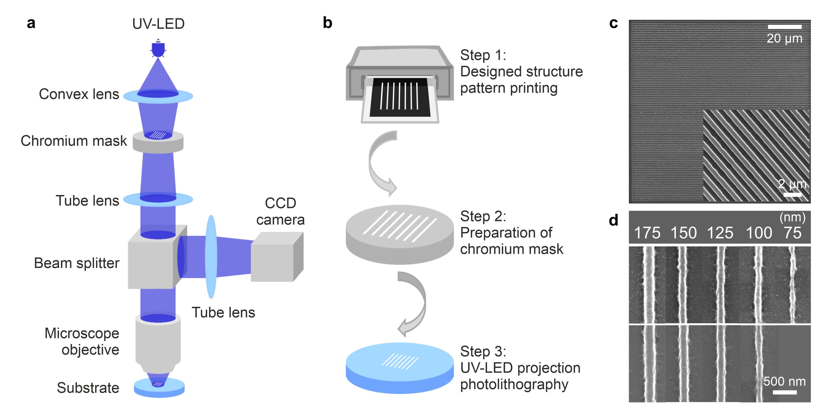
In a new Light: Advanced Manufacturing paper, scientists Dr.-Ing. Lei Zheng et al. from the Leibniz University Hannover have developed a low-cost and user-friendly fabrication technique, called UV-LED-based microscope projection photolithography (MPP), for rapid high-resolution manufacturing of optical elements within seconds. This approach transfers structure patterns on a photomask to a photoresist-coated substrate under UV illumination.
The MPP system is based on standard optical and optomechanical elements. Instead of a mercury lamp or a laser, an extremely low-cost UV-LED with a wavelength of 365 nm is used as the light source.
The researchers developed a preceding process to obtain the structure-patterned chromium mask required in MPP. It includes structure design, printing on a transparent foil, and the pattern transfer onto the chromium photomask. They established a lithography setup for the preparation of photomasks as well. Structure patterns printed on the transparent foil can be transferred to a chromium photomask with this setup and a subsequent wet-etching process.
The MPP system can fabricate high-resolution optical elements with feature sizes down to 85 nm. This is comparable to the resolution of much more expensive and complex fabrication methods, such as multi-photon and electron beam lithography. MPP could be used to fabricate microfluidic devices, biosensors, and other optical devices.
This fabrication approach developed by the researchers is a significant advancement in the field of lithography for the rapid and high-resolution structuring of optical elements. It is particularly well-suited for applications where rapid prototyping and low-cost fabrication are important. For example, it could be used to develop new optical devices for biomedical research or to prototype new MEMS devices for consumer electronics applications.
More information:
Lei Zheng et al, Feature size below 100 nm realized by UV-LED-based microscope projection photolithography, Light: Advanced Manufacturing (2023). DOI: 10.37188/lam.2023.033
Citation:
A low-cost microscope projection photolithography system for high-resolution fabrication (2023, November 30)
retrieved 30 November 2023
from https://phys.org/news/2023-11-low-cost-microscope-photolithography-high-resolution-fabrication.html
This document is subject to copyright. Apart from any fair dealing for the purpose of private study or research, no
part may be reproduced without the written permission. The content is provided for information purposes only.
Denial of responsibility! TechCodex is an automatic aggregator of the all world’s media. In each content, the hyperlink to the primary source is specified. All trademarks belong to their rightful owners, and all materials to their authors. For any complaint, please reach us at – [email protected]. We will take necessary action within 24 hours.

Jessica Irvine is a tech enthusiast specializing in gadgets. From smart home devices to cutting-edge electronics, Jessica explores the world of consumer tech, offering readers comprehensive reviews, hands-on experiences, and expert insights into the coolest and most innovative gadgets on the market.


