× close
Two-terminal devices are electronic components connected to electrical circuits via two electrical terminals. Although these components are the key building blocks of most existing devices, they can limit a system’s performance and functions.
Researchers at the University of Science and Technology of China (USTC)’s iGAN Laboratory led by Prof. Haiding Sun and other institutes in China recently developed a new three-terminal diode that can both emit and detect light.
This diode, presented in a paper published in Nature Electronics, could open new possibilities for the development of highly performing wireless communication and light-driven computing systems.
“Inspired by the limitations inherent in traditional two-terminal devices (e.g., p–n diode), we, sought to enhance the functionality and performance of conventional optoelectronic devices,” Haiding Sun, lead author for the paper, told Tech Xplore.
“Our team developed a multifunctional device that serves as an advanced light emitter as well as a photodetector, significantly enhancing their capabilities in the implementation of optical wireless communication (OWC) and paving the way for optoelectronic logic gates (OELGs) for advanced optically controlled computing technologies.”
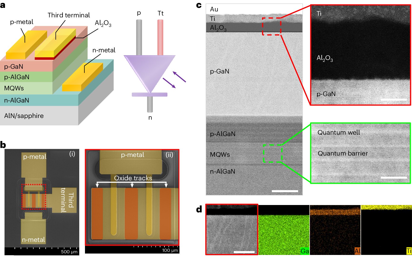
The three-terminal diode designed by Sun and his team combines a traditional gallium nitride-based p–n diode with a newly introduced third terminal. This third terminal is comprised of a metal/Al2O3 dielectric layer directly applied to the p–GaN layer.
“In the operation of primary mode as a light emitter, the device modulates light intensity by adjusting the bias applied to the third terminal, which significantly increases the modulation bandwidth,” Sun explained.
“When functioning as a photodetector, the device utilizes both voltage and incident light as inputs to establish reconfigurable NAND and NOR optoelectronic logic gates, showcasing its versatility.”
The new light emitting and detecting diode developed by the researchers could be particularly advantageous for the development of OWC systems. In initial tests, the three-terminal diode was estimated to enhance modulation bandwidth by more than 64%, which is a substantial improvement over current OWC systems employed with classic light-emitting p–n diode.
“The ability to switch seamlessly between emitter and detector modes also provides a versatile and dual-functional device architecture for developing faster, more efficient, and reliable data transmission methods,” Sun said.
“We believe this innovative approach holds promise not only for GaN materials but could also be adapted to other semiconductor platforms, paving the way for the development of multifunctional and integrated electronic and optoelectronic systems (e.g., integrated photonics).”
The diode developed by this research team could eventually be used to fabricate OWC technology that can transmit data at higher speeds, as well as innovative optically driven computing systems. Meanwhile, Sun and his colleagues are building on their initial promising results and exploring potential techniques to further enhance their diode.
“Our next studies will focus on refining the performance and exploring integration with other optoelectronic materials and systems,” Sun added. “The goal is to develop compact, multifunctional integrated optoelectronic systems that could revolutionize various technology sectors, particularly in high-speed data communications and advanced computing platforms.”
More information:
Muhammad Hunain Memon et al, A three-terminal light emitting and detecting diode, Nature Electronics (2024). DOI: 10.1038/s41928-024-01142-y
© 2024 Science X Network

Wanda Parisien is a computing expert who navigates the vast landscape of hardware and software. With a focus on computer technology, software development, and industry trends, Wanda delivers informative content, tutorials, and analyses to keep readers updated on the latest in the world of computing.


