While the speed of light in a vacuum is a constant and cannot be exceeded, it can be slowed down in other media, meaning it can be manipulated more – which is crucial in designing photonic chips.
“When light is slowed down, the energy density of the light increases,” said Dr Li Guangyuan, a researcher of optical engineering at the Shenzhen institute who led the study.
“This means that with the same device length, the effective distance for the light to interact becomes longer – essentially enhancing the performance of a photonic device.”
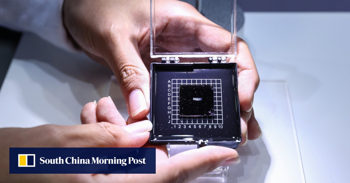
Li’s team designed a photonic chip in a way that slowed down the light by more than 10,000 times. They said this was done with a greatly reduced loss of energy, which was only about 20 per cent of the loss seen in previous attempts.
The current mainstream method to control light speed relies on metasurfaces – artificial materials made up of nanostructures. When light strikes these nanostructures they resonate, altering its amplitude and phase.
But the material absorption and scattering of light produced by these artificial atoms can lead to a loss of light that reduces the lifespan of photons, limiting the extent to which the speed of light can be slowed.
To get around this, Li’s team made improvements to the materials used and the structural design.
“In terms of material selection, we opted for materials with low or even no absorption loss at the wavelengths of interest,” Li said.
“For instance, metals have strong absorption in the infrared spectrum, so we used lossless silicon materials. However, silicon absorbs strongly in the visible light spectrum, so in those cases, we used transparent materials like silicon nitride or titanium dioxide.”
China’s semiconductor industry weathers tough year amid tighter US sanctions
China’s semiconductor industry weathers tough year amid tighter US sanctions
For the structural design, the researchers improved upon a concept called surface lattice resonance, which involved a periodic surface pattern to prevent the loss of energy.
“We designed a periodic surface structure of 100-nanometre silicon nanodisks,” Li said.
“This design shifts the light’s path from inside the nanostructures to their surfaces, greatly reducing material absorption loss. Also, some photons that are lost due to scattering are recaptured by adjacent structures, rejoining the propagation process and extending the photon’s lifespan.”
Li said the technology could also reduce manufacturing costs for photonic chips and increase their applications.
“By using metasurface technology, photonic chips can be as thin as stickers or building blocks, allowing for functional stacking,” he said.
Using that technology, researchers have been able to use photonic chips for devices like sensors, lasers and LEDs in recent years.
“The performance of these photonic devices is limited by the very limited interaction length in such ultrathin photonic chips,” Li said. “By using the slow light effect, the performance can be significantly improved.”

Wanda Parisien is a computing expert who navigates the vast landscape of hardware and software. With a focus on computer technology, software development, and industry trends, Wanda delivers informative content, tutorials, and analyses to keep readers updated on the latest in the world of computing.


